

JEDEC JESD22-A106 Compliance: Ensuring Semiconductor Reliability Through Temperature Shock Testing
Publish Time:2026-08-11Views:()
In the semiconductor industry, JEDEC standards are the common language between chip designers, foundries, assembly houses, and end customers. Among these, JESD22-A106 defines the temperature shock test — a critical reliability screen that exposes weaknesses in die attach, wire bonds, and package interfaces before products ship.
The Problem: Solder Joint and Wire Bond Failure Under Thermal Shock
Semiconductor packages contain multiple interconnection technologies: die attach adhesive or solder, wire bonds or ribbon bonds, and solder balls or columns. Each interconnection must survive not just the operating temperature range, but the rapid temperature transitions that occur during manufacturing (reflow soldering), testing (burn-in), and field use (power cycling in automotive or industrial environments).
When temperature changes rapidly — for example, from +125°C to -40°C — the different materials in the package contract at different rates. Solder joints, which are already brittle at low temperatures, develop tensile stress at the package-substrate interface. Wire bonds experience flexure fatigue at the heel. Die attach layers develop shear stress that can cause cohesive or adhesive failure.
JEDEC JESD22-A106 is designed to accelerate these failure mechanisms in a controlled, repeatable manner.
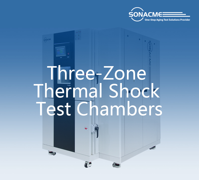
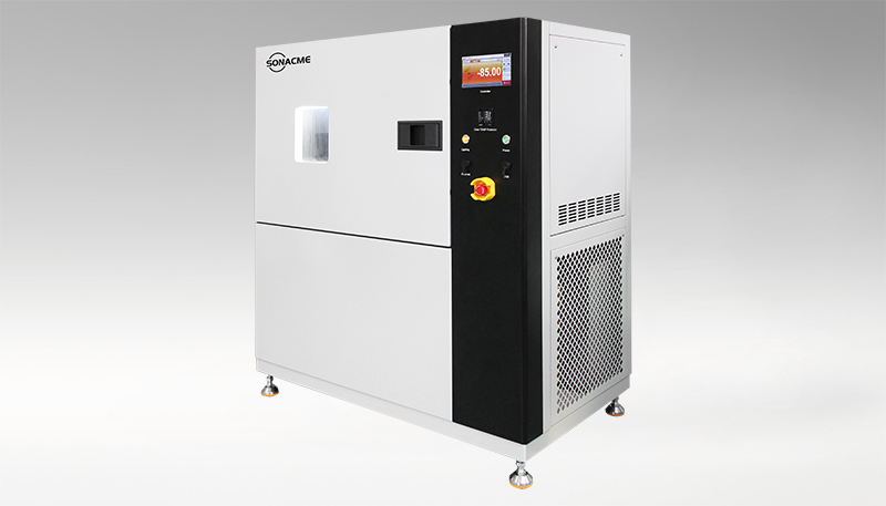
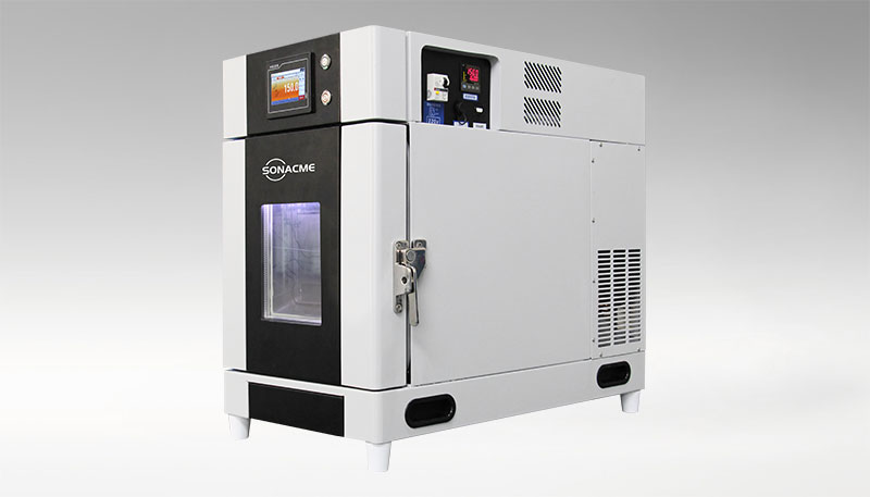
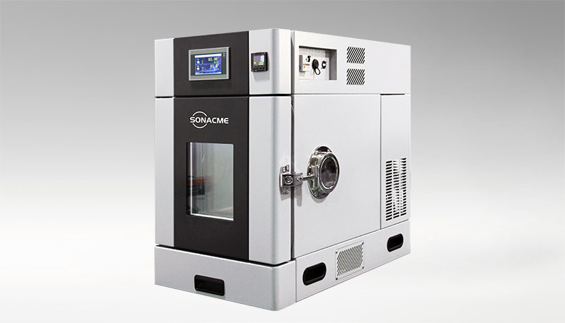
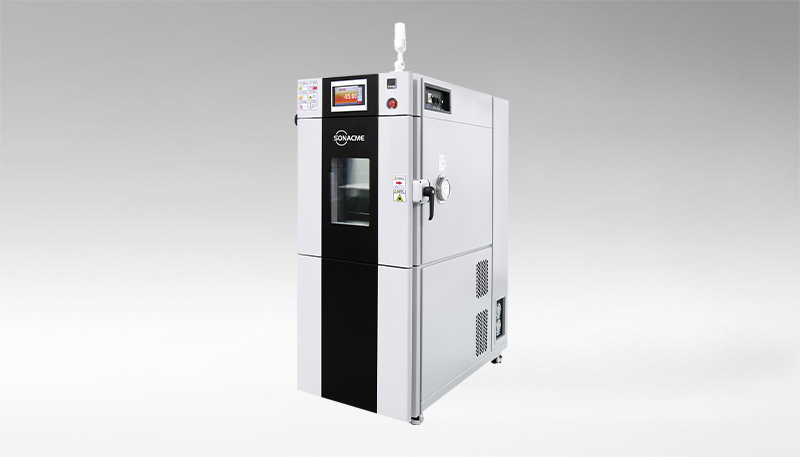
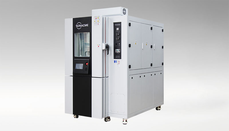
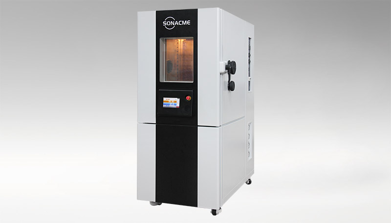
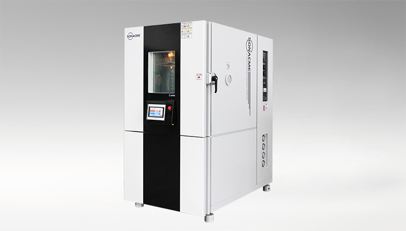
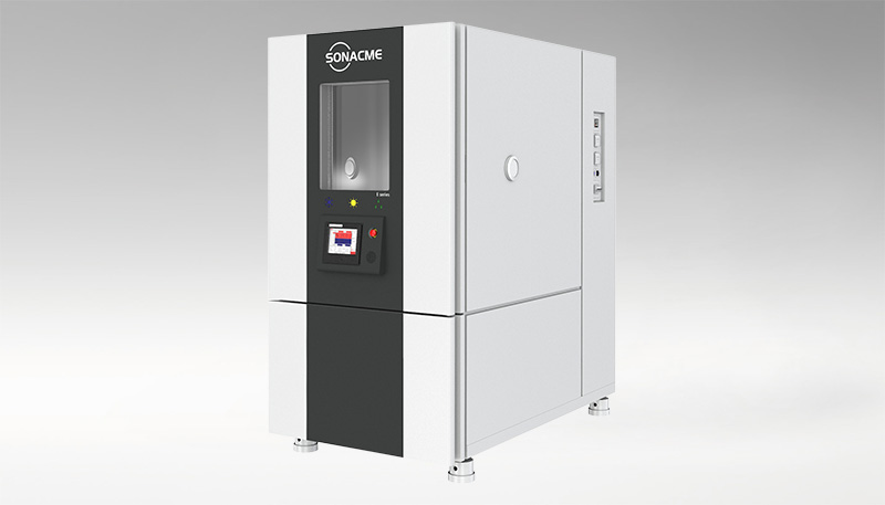
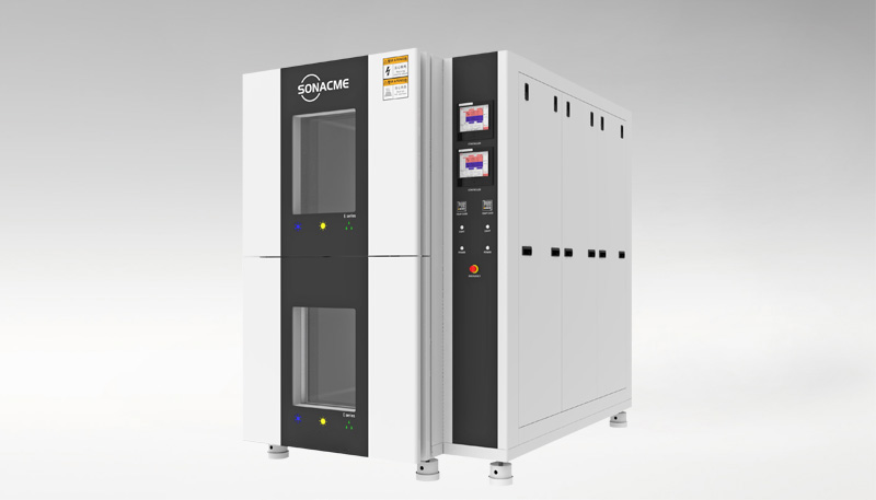
SONACME Three-Zone Thermal Shock Test Chamber: Meeting JESD22-A106 with Precision
SONACME's Three-Zone Thermal Shock Test Chamber uses a damper-switching mechanism to expose specimens to hot and cold air in alternating cycles, without physically moving the specimen. This design is particularly suited for JESD22-A106 testing where controlled air-to-air transition is specified.
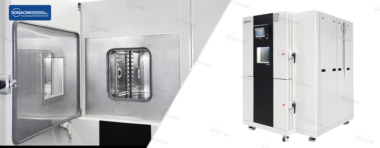
Key Technical Parameters
High Temperature Range: +60°C to +200°C
Low Temperature Range A: -40°C to 0°C, B: -55°C to 0°C, C: -65°C to 0°C
Heating Time Ambient to +200°C within 15 minutes
Cooling Time Ambient to -75°C within 40-50 minutes (model dependent)
Volume Options: 50L to 1000L
Internal Material: SUS304 Stainless Steel, 1.2mm, full welding
Insulation: 100mm polyurethane foam
System: Damper switching (three-zone design)
The three-zone design offers distinct advantages for JESD22-A106 compliance:
- No mechanical transfer shock: The specimen remains stationary, eliminating the risk of mechanical damage that could confound thermal shock results
- Precise transition control: Damper switching achieves sub-10-second transition times consistently
- Uniform exposure: Controlled airflow ensures all specimens receive equivalent thermal exposure
Test Protocol: Implementing JESD22-A106 in a Semiconductor Lab
A recommended JESD22-A106 test protocol using the SONACME chamber:
1. Sample preparation: 45-77 devices per lot (per JEDEC sampling guidelines), with pre-test electrical screening
2. Condition selection: Condition B (+125°C / -55°C) for commercial/industrial devices; Condition C for automotive/military
3. Cycle execution: 200 cycles minimum, with interim electrical reads at 50, 100, and 150 cycles
4. Failure analysis: Wire bond pull/shear, die shear, cross-sectioning, and SAM for any failures
The SONACME chamber's self-developed controller allows programming of up to 10 test procedures with 15 segments each, enabling automated multi-condition testing without operator intervention.
Why JESD22-A106 Matters for Modern Semiconductor Packages
As the industry moves to heterogeneous integration — combining logic, memory, and passive components in a single package — the number of material interfaces and interconnection types increases dramatically. Each new interface is a potential failure point under thermal shock. JESD22-A106 provides the standardized framework to evaluate these interfaces systematically.
Whether you are qualifying a new flip-chip BGA, validating a chiplet interposer design, or screening a legacy QFP package, SONACME's thermal shock chambers provide the precision, compliance, and reliability that semiconductor manufacturing demands.
Contact SONACME Technology to learn how our thermal shock test chambers can support your JESD22-A106 compliance testing program.
Latest News
-
IEC 60068-2-14 Nb: Rapid Te...
JEDEC JESD22-A106 temperature shock testing complian...
-
MIL-STD-810 Method 503 Ther...
JEDEC JESD22-A106 temperature shock testing complian...
-
IEC 60068-2-14 Na/Nb Testin...
JEDEC JESD22-A106 temperature shock testing complian...
-
Meeting ISO 26262 Standards...
JEDEC JESD22-A106 temperature shock testing complian...
-
IEC 60068-2-38 Environmenta...
JEDEC JESD22-A106 temperature shock testing complian...
-
Essential reading for autom...
JEDEC JESD22-A106 temperature shock testing complian...
+86-180 2704 9206
Tel:+86(0769)83234966
E-Mail:info@sonacme.com
Contacts:Marcia/+86-180 2704 9206
Add:Building 7, No.310 Songbai Road, Liaobu Town, Dongguan City, Guangdong


 +86-180 2704 9206
 WhatsApp:+86-180 2704 9206
 info@sonacme.com